PCB Assembly Service Review: ALLPCB China
Ordering Assembly Service From a China Fab House: All The Details (Really Everything!)


How does the PCB Assembly process work? How long does it take? What can go wrong? How much will I pay for the service?
Unfortunately, it is hard to find all this information online. This led me to experiment myself with a real-life use case and share the results in this series of blog posts, so you can learn too.
Arduino with USB Type C ?
After being frustrated with the bulky USB Type A cables that are currently used for Arduino Uno, I decided it was time to upgrade our little friend with a USB Type C connector. Sure, you can find Arduino Uno compatible boards with Micro USB, but wouldn't it be more fun if you didn't have to try at least 3 different times until the cable plugs in?
View post on imgur.comThis board includes 42 SMT components (as well as some through-hole parts, but these are easier to do manually). The USB Type C connector and ATmega16U2 chip are the most challenging to solder manually:

So, instead of getting a stencil, smearing the messy solder paste, manually placing all the components using tweezers, and baking on a hot plate, I decided to use this board as the test case for comparing different PCB assembly houses in China.
Printed Circuit Board Assembly ?
Before we dive into the specifics of my experience with ALLPCB, here is a quick review of how the PCB assembly process works:
- You design your PCB. I usually use KiCad for that, sometimes also EasyEDA.
- Once your PCB design is ready, you export it in a format called Gerber.
- You create a Bill-of-Materials (BOM) that contains a list of all the components that go on your board, their quantity and supplier part number / link.
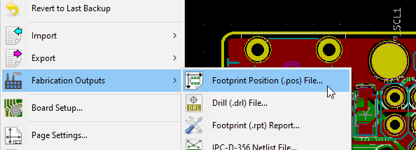
Some assembly houses require specific BOM file format, but most just accept any kind of CSV / Excel file, as long as they can find the relevant information. - You export a Pick-and-Place file from your PCB design software. This file contains information about the location and the orientation of each component.
- You send all the files (Gerber, PCB, BOM) to the factory. They review it, outline any issues, and eventually send you a quote. Most of the assembly houses can also purchase the components for you, and the quote also includes the price of the parts.
- You pay, and the assembly house orders the components and start making the PCB.
- Once the components have arrived and the PCB is ready, they program the pick-and-place machine. At this stage, they will probably contact you if there is a problem (such as a component that doesn't fit well in the PCB footprint).
- If everything goes well, the PnP machine assembles the boards (you can ask for a photo to make sure all looks fine), and then the through-hole components are soldered.
- The boards can also be programmed with a HEX file you supply, for extra charge (usually around 0.2-0.5$/unit)
- The assembled boards are packed and shipped to you. The PCB factory may also send you a photo of the assembled board to confirm just before shipping.
As you can see, this is a pretty long and involved process, and there is a lot of room for errors. So how did it go with ALLPCB?
Online Quote, Read The Fine Print ?
ALLPCB, like many of their competitors, have an online quote system, where you can input information about your design and the number of components to assemble and get an instant quote.
When you go to their PCB assembly page, you are greeted with a hard-to-miss offer of only $29.99 for PCB assembly, with just 24 hour turn-around time:

Note, however, that this is just the price for the assembly service, and you will have to pay for the PCB separately, as well as for the components. Furthermore, you may be surprised when you get a different number after you input your order parameters:

If you read the fine print, you will find that the special prices only applies for orders which meet certain criteria:

In my case, the board quantity was fine, but the sum of solder joints was way too big: (156*53) = 2029, which is way greater than the allowed 400.
I changed my order parameters to stay within the limits: changed to board quantity to 2, and cut down some of the DIP components (I could solder these myself), so that I stay below the limit. The assembly price went down to 29.99$, as promised.
Placing The Order ?
Once I was happy with the price, I added my order to cart, and was asked to upload the BOM and Pick & Place files:

Since they didn't say anything about the format of the files, I just went with the format I had. The BOM was a spreadsheet which looked like this:

While the Pick & Place file was exported directly from KiCad:
But then, when I tried to upload this file to the ALLPCB site, I got an obscure error message in Chinese, and the file didn't go through:

I couldn't translate this message, as it disappeared as soon as I clicked somewhere in the page, and so, I sent an email to their support (never got a reply), and tried different things until eventually I figured it out: KiCad generates a CSV file, and their interface would only accept xlsx files. Not very user-friendly.

After figuring this out, my order went through. I also ordered the PCB (white one with a black silk screen), added the Gerber files, and checked out. The total sum was $60.02, which also included $0.99 PCB price, $27 shipping, and some PayPal fee. Not too bad...
OMG, This Is Too Expensive! ?
I waited and about 12 hours later got an email from ALLPCB sales representative saying:
I noticed that you placed an assembly order and I am sorry that I forget to quote you the price of Components.
I would quote for you ASAP!
6 hours after I also got the quotation for the components (remember, the PCBA price is only for the label, components are quoted separately):
Thank you for your waiting. I am always working on quote for you a favorable price.
Please kindly check the components quotation sheet in the attachment.
Pls notice: In yellow color, some remarks need your confirmation if it's OK for you.
Their price, however, didn't seem favorable at all:

However, a better inspection revealed that their engineer thought the number of pads was the quantity of each component, so instead of ordering just 1 ATmega16U2 chips per board, she thought we'd need 32 (I don't see how this makes any sense), and quoted accordingly.

I added a new Quantity column, and also confirmed the alternative parts she suggested, and sent her the new BOM. She quickly confirmed her mistake:
Oh dear,
Sorry for my mistake and I am working on quote you the updated price.
It wasn't until a day later when she sent me a new price, 19.70$, which now also made sense. I paid the difference (total of $22.66, due to the added PayPal fees), and finally my order was confirmed.
Design Problems, We Can't Solder That ?♂️
About 2 hours after paying for the parts, I got another email outlining a problem with my design:
Thanks for your order.
There is one EQ need to be confirmed.
As for the marked holes, pls confirm if they are DIP or vias.
If DIP, the space of these holes are too narrow, pls enlarge the space.
If vias, it shoudn't change and we will arrange to fab it soon.
They also sent a picture showing the holes in question:

Apparently, the leads of the USB Type-C receptacle I used were too challenging for their manufacturing facilities. I sent them a photo of the connector, saying that they could skip soldering these holes if it was a problem, and I'd solder myself once the board arrives.

However, they responded they couldn't fabricate a PCB with these holes:
Thanks! We could solder these holes for you. But these DIP holes are too narrow to fabricate it.It will be appreciated if you could enlarge the space between these holes. So that we could make it for you as soon as possible.
Oh well... At least they told me about it before manufacturing the PCBs.
I looked for a different connector, one that had no though-hole pins, and updated my board design accordingly. Just as I emailed them the new Gerber files, I got another email saying that they had a problem with my silk screen (the text that is printed on the board):
Dear,
In the meanwhile, could you pls provide the complete silkscreen for us?
Also, in your pick and place file, the part X1 ZU4 has been missed, could you send the updated file to us?
They also attached a screen shot of the silk screen, which looked fine to me:

It took another back-and-forth email to figure out what they really needed. They wanted me to include a Factory Fabrication Gerber file, which contains the Designator (part identifier) for each of the components on the board, so they could place it.
These files are not exported from KiCad by default, so you have to explicitly ask KiCad to include the files when generating Gerbers:

You only need to do this if your Silk Layer does not include the Designators. In my case, including them in the Silk Layer would make the board not-as-pretty:

And so, I sent them another iteration of my Gerber files, as well as updated pick-and-place file with the positions of the Through hole components they requested, X1 and ZU4.
KiCad doesn't include through-hole component in the Pick-and-Place file, so I had to define them as SMD components first:

And finally, 3 days after initially placing my order, they told me they'd start manufacturing it:
YES, finial worked. Thanks for your new gerber file. We would fab your PCBs with your new file as soon as possible.
Hooray!
I checked their website periodically and tracked the PCB fabrication progress:

Wrong Part Numbers ?
The email went silent for about a week, and then, they told me they received all the parts but there were some issues:
1: ON1--the link you provide, our staff make a mistake and purchase the wrong one, and we would take responsibility to you and re-purchase them then assembled. But the delivery time will be longer. Can you accept it?
2: X2--U262-241N-4BV60 (USB) the compoents you provide has the THT joints but on your PCBs, there were no holes. Pls kindly advise, do we need to repurchase or leave it alone.
3: TX1. RX1. L3. ON1, pls mark the polarity, like draw "+,-" in picture. Or is the pic show right?

So the "ON" LED was their mistake. What happened with the USB Type C connector? It turns out I forgot to send them the new part number when I switched to SMT-only connector, so they ordered the original one, with the through-hole pins:

Furthermore, the PCB didn't include any indication about the LED polarity (my bad, I should have added it to the Fab layer), so they took some wild guesses. They figured out TX1 and TX2 correctly though!

Since they made a mistake with the part number, they offered to repurchase the missing LED and the SMT-only USB C connector without any additional charge, but they advised it'd delay the assembly:
We would start to repurchase the ON1 and X2. They would both need a long time to repurchase, hope you can understand and we would arrange the assembly once the rest of them arrived!
Lesson Learned - Whenever making any last-minute changes to the design, make sure to update and resend both the BOM and the P&P file, to ensure no missing parts.
Confirm Some Issues? ?
After 5 more days, I got an email that said:
Regarding our assembly item A_H56974S5_3, We need your help to confirm some issues.
Hmm... even more issues? However, when I opened the attached link, I saw a photo of the assembled board, which looked pretty good:

Overall, the board looked good!
There were some unpopulated parts (the female pin headers, the ICSP connectors, and the Reset button), but I intentionally left them out to get the cheaper assembly price.
In addition, two resistors were missing (below and next to the USB connector). However, I checked and it was my bad - I forgot to include them in the BOM (they did appear in the pick-and-place file, though).
The most disappointing part, for me, was the Wokwi's logo was missing. It turns out that I accidentally deleted it when I exported the Gerber files for the last time, when I added the missing Fab layers. Bummer!
Anyway, I was eager to receive and test out the boards, so I confirmed that order and waited eagerly for the boards to arrive.
I Got The Whole Board In My Hands! ?
When I got the package, I was surprised by the big box that arrived. It contained many small anti-static bags with tiny SMD components:

When you order a PCB Assembly service, the factory usually purchases more parts than are needed, for several reasons:
- Some parts have minimum order quantity (MoQ). For instance, I used only two 22Ω resistors in my design, but the minimal amount you can buy is 100. This makes low-volume PCBA orders not very cost-effective.
- The Pick and Place machines sometimes miss a part or two, so it's better to have some extra parts rather than having to stop the machine, purchase a missing part, wait for it to arrive, and then restarting the assembly process.
Most importantly, the package had the assembled PCBs (along with some extra, unpopulated PCBs):
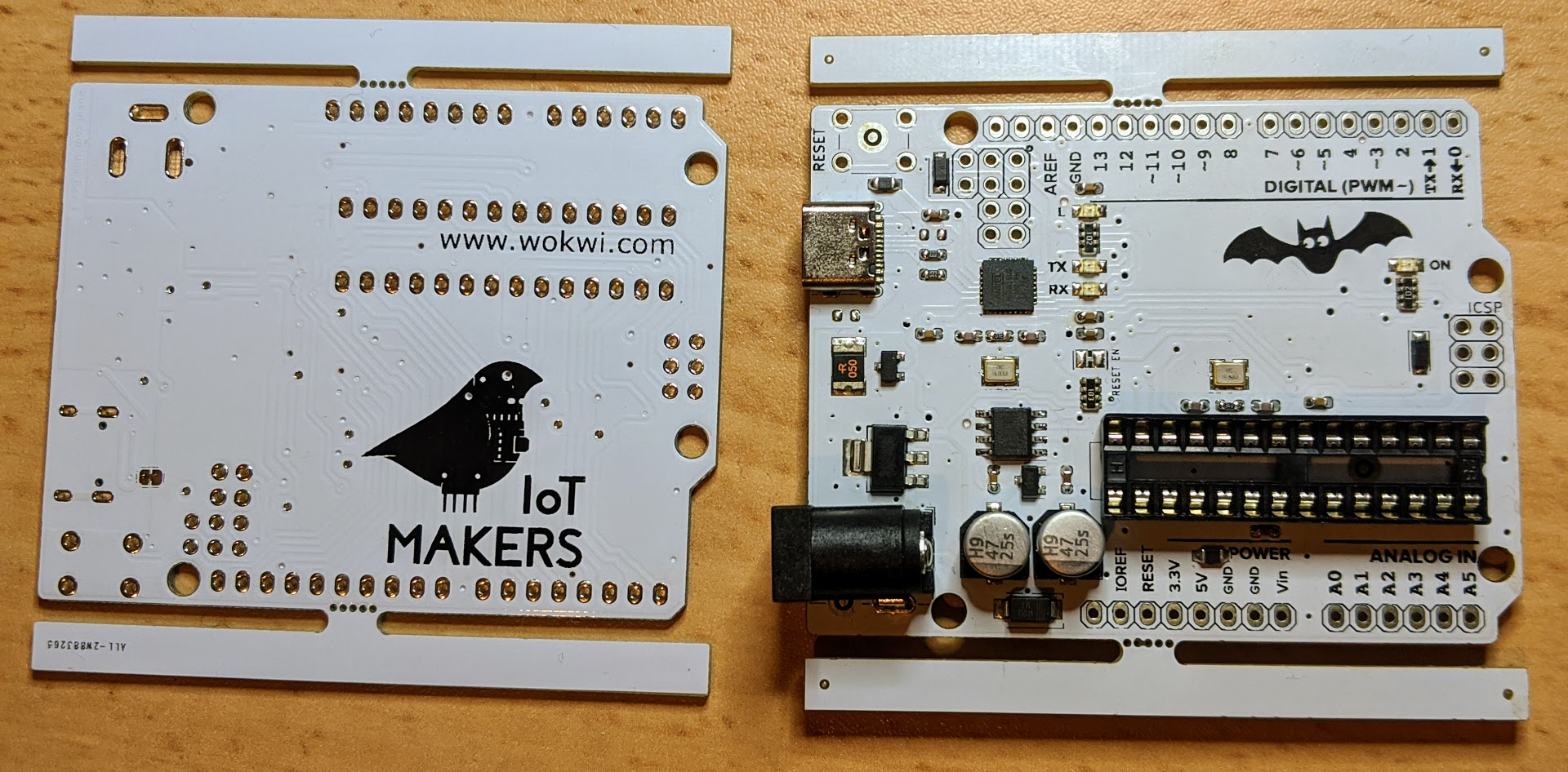
You can spot the IoT Makers Meetup logo on the back of the PCB, and you may have also noticed the two square bars, one on top and one at the bottom, that are connected by small tabs to the edges of the board.
PCB fab houses usually add the order number on the board. In order to avoid this, I usually design my boards in form of a panel, so the order number gets printed on these bars (you can see it on the bottom-left corner of the photo above). I then remove these panel edges using flat pliers, and file the edges of the board after breaking away the tabs.
After adding the missing resistors, plugging in an ATmega328p chip, and soldering the reset button, ICSP headers, and female headers (the ones where the shields go), I connected it to my computer and run a quick test. It worked like a charm!
One annoying thing, though, the assembled PCB had a sticky feeling. It probably has to do with the assembly process, as the unpopulated PCB aren't sticky at all. Cleaning with alcohol helped, though.
Summarizing The Experience
The whole manufacturing process of the boards took 14 days (+ 3 days for shipping) and costed total of $87.68 (including shipping, PayPal fees, etc).
Overall, the process felt too manual and error-prone to me. Communication was a challenge, and I had to figure out some of the bits myself (like which layers to export out of KiCad, how to format the BoM and PnP files, the issue with the USB type C connector).
I believe that without all the back-and-forth emails and the factory ordering the wrong part numbers, it would only take a week or so to produce these boards.
I learnt several lessons that I'm going to apply in my future orders: including a Quantity column in the BOM, exporting the Fab layers from KiCad, checking the stock status for all parts in my BOM just before ordering (LCSC has a BOM tool that can do that), double checking that the BOM and Pick-and-Place files both have the same components, and looking at my exported Gerbers twice when I make any last-minute revisions.
Despite all the challenges, at the end of the day, I got a working product in a reasonable time, and the team at ALLPCB did pretty good job in spotting potential issues and working out viable solution together with me, and I can conclude this experiment as a success.
I hope that this write-up will help others who are going on a similar journey. I'm now checking other PCB Assembly fab houses, and plan to publish my findings over the next few weeks.
Thank you for joining me here and reading on my adventures. If you like this kind of content, I invite you to join our mailing list and be the first to know when we publish some new content: