A Practical Guide to Designing PCB Art
How to Turn Custom Artwork into Fun and Functional Electronic Circuit Boards!


How to Turn Custom Artwork into Fun and Functional Electronic Circuit Boards!
Printed Circuit Boards (PCBs) are literally all around us: nearly every consumer electronic good contains a PCB, and more and more we see people designing their own to use in their DIY electronics projects — I’ve certainly designed a few myself for all kinds of funky projects!
When I started working on ng-beacon, I realized that you could do even more with PCBs: you could make them “art,” too! This led to designing a heart-shaped keychain light for my girlfriend’s birthday, as well as an ‘angry panda’ I made for my friend Pavel 'PK' Kaminsky (meant to resemble the logo of his CrossFit club):
My girlfriend had a birthday, so I designed this small PCB for her ???#DiY #Makers @oshpark pic.twitter.com/2sn4akLro9
— Uri Shaked (@UriShaked) March 21, 2017
I designed an angry panda circuit board, really happy with how it came out! thanks @PCBWayOfficial @kicad_pcb ? pic.twitter.com/ZJBNsK6g1c
— Uri Shaked (@UriShaked) August 18, 2017
But why would you want to make art out of a PCB?
Well, for starters, they are dirt cheap to have made (they can get as low as $5 for a batch, even including worldwide shipping), and the manufacturing process includes many steps and processes we can take advantage of in our designs. If you wanted to build them yourself — ordering a CNC machine, silk screen, etc. — you’d be spending quite a lot on setup, but the nice thing about PCBs is that you can have them made for you with everything included for very affordable price with a streamlined ordering process.
Beyond the logistical advantages, custom art PCBs can make great gifts, conference badges, or “smart decorations” — not to mention they can make your next electronics project look that much cooler. And isn’t engineering in part about combining function with form?
When I was beginning to play around with PCB art, I discovered that there weren’t any good end-to-end tutorials which took you from a graphics file through all the steps to get a manufactured PCB. So, I experimented with different tools and methods, and decided to write my own!
PCBs 101
Before we dive in, let’s first take a moment to get a grip on what exactly makes up a PCB, and what happens during the PCB manufacturing process. Having a good understanding of what we’re working with will give us a better idea of what crazy fun things we can do with them!
What’s in a PCB?
You can think of a PCB like a hacker sandwich: PCBs are essentially a bunch of materials pressed together and etched/marked so that, when pieces are soldered to them in the correct way, they do what we want them to.
The base material is called “FR4,” which is a kind of fiberglass with green-yellow color. On top of that (and sometimes on both sides!) there is a copper layer, which serves as the board’s conductor, replacing the wires you’d otherwise need between the components. This is then plated with either a thin solder, a process called HASL, or thin gold layer, a process called ENIG — this plating is what makes PCBs easier to solder, as well as ensures that the copper in your board doesn’t corrode.
Next, we have the “solder mask.” This solder mask is what helps us make sure we’re soldering our components to the correct places, and that the current between them goes where we want it to (and importantly, not where we don’t!). The solder mask is also what gives the PCBs their color:

Common colors for solder masks include red, green, yellow, blue, black, white, and purple. As you can see in the photo above, however, there’s also some lettering and design on top of the solder mask. This is the “silk screen” layer (which is now most often laser or ink jet printed instead of literally silk screened), which is usually white, unless you’re printing on a white board (in which case it’s black).
The silk screen is traditionally used to mark where various components go and what they’re supposed to do, but in our case they can also help us make the most out of our artwork!
So to take my Panda as an example, we start with a piece of FR4, add a copper layer, and then plate it with a solder (HASL) finish, which you can see it on the nose / tongue which has a metallic shiny finish.

On top of that, there’s a the black solder mask — everything black you see above is actually the solder mask. Finally, I used the white silk screen to make the panda’s face, and I also used it to print the GitHub URL on its back:

If you look closely at the top side, however, you will notice there are actually two different shades of silk screen: there is a slightly darker shade on the side of the face. I achieved this by using a copper layer below the silk screen, which will give the silk screen a slightly darker shade.
If you’d like to learn a little more detail about what makes up a PCB, SparkFun has a nice article about it.
How are PCBs Manufactured?
A detailed look into the PCB manufacturing process could take up a whole post all by itself, but in order to get started making PCB art, we (thankfully) just need the basics.
Essentially manufacturing a PCB comprises of the following broad steps:
- Transfer the PCB design to photo film(s). This process can happen in a number of different ways depending on the type of process the manufacturer chooses to use, but basically it involves printing the desired PCB schema onto one or more films which will then be transferred onto the actual board, with different films for each layer of the PCB.
- Transfer design from film(s) onto the copper. This is actually a pretty complicated, multi-step process, but the general idea is that you clean the copper, transfer over the design from the photo films, zap it with UV light to keep the copper you want, wash away the unwanted copper with chemicals, and then use a combination of fusing, drilling and plating to make sure the PCB can conduct electricity the way we want it to.
- Apply the solder mask. Again, the manufacturer uses special inks and UV lights to apply the solder mask to the board, which is then cured in an oven.
- Apply the surface finish. In order to ensure easy solderability, the manufacturer will chemically plate the PCB with gold or silver, which attaches itself to the copper exposed from the solder mask.
- Silkscreen the PCB. This is when the relevant electrical information is printed onto the PCB, or in our case, where we have an opportunity to add a bit more design!
- Test and cut. Finally, before the PCB gets shipped out to the users, the manufacturer will test the actual circuits in the PCB, and then cut out the individual boards from the group in which they were made.
The above is a very abridged version of the PCB manufacturing process, which can be rather complex! Still, it’s not so complex that people don’t occasionally make their own PCBs, but for our purposes, we’ll stick with established manufacturers.
For a more detailed explanation of the process, this video does a pretty good job, as does this walkthrough from PCBCart.
From Digital Art to Physical Object: DiY PCB
So now we know how PCBs are made, let’s make one! We will use the heart example — which is slightly easier — and then I will give you some hints about the Panda one (if you want to try it).
For our walkthrough, we’ll only use free tools: Inkscape, KiCad, and a python script called svg2mod.
Inkscape is a vector graphics editor — similar to Adobe Illustrator. In fact, if you have an Illustrator vector file, and want to use it as a basis for your PCB artwork, you can export it to SVG format and then open it with Inkscape.
I used to use a program called Eagle to design PCBs as hobbyist for several years, but after making a few projects, I began to appreciate how hard Eagle makes it to import and manipulate shapes. So I found KiCad, a free alternative, offers a much more streamlined process for designing art PCBs, and that’s what I use now — use the right tool for the job as we software engineers love to say.
Creating The Base
First of all, we create all the board elements in SVG format. For this tutorial, we will start with the heart shape — you can download mine here (click the “Raw” button, the Ctrl+S to save it) or just draw one yourself (or another option). You can use different artwork, of course, but I will stick with the heart for this tutorial.
If you choose to draw the shape yourself, make sure that the stroke width is 0.1mm (set it with Ctrl+Shift+F then “Stroke Style”), otherwise the shape dimensions will be slightly changed when you import it to KiCad.
Open the SVG file in Inkscape. We will use the heart as the outline (i.e., the shape) of the board. If you want any holes in the board (such as the eyes, in case of the Panda), you would draw them at this step.

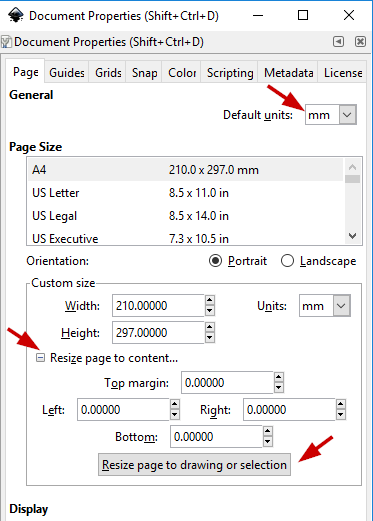
When you’re working on the file in Inkscape, make sure you use the real-world measurement units such as mm, cm inches for units — I used mm, and set the size of the heart to be about 30mm. To make sure the document is resized to contain the heart — “File -> Document Properties…” then click on “Resize to page content…” and then “Resize to drawing or selection”.
Finally, before we can use this heart shape in KiCad, we need to flatten any Bézier curves we might have, as KiCad doesn’t know how to deal with those. To do this, select the heart shape and go to the “Extensions” menu -> “Modify Path” -> “Flatten Beziers…”. Then enter a Flatness value — the smaller the value, the more accurate the result will be. I found that 0.1 yields good results.

Note: If you’re using a Mac, you may see this error in Inkscape, depending on your installation: “The fantastic lxml wrapper for libxml2 is required...” If you encounter this error, you might try this workaround, or failing that, this.
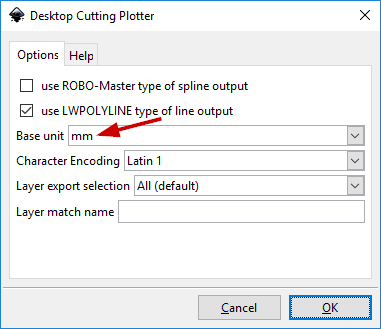
Great! So we’ve got our heart set up as the edge shape of the board , and we can now export it into DXF file (the type of file we need to import our shape into KiCad). To do so, select “Save copy as…” in the file menu and select “Desktop Cutting Plotter (AutoCAD DXF R14) (*.dxf).” Let’s save the file as heart.dxf for simplicity. When exporting, make sure to select the base unit as “mm”:
Now, open KiCad, create a new project, and then open “Pcbnew” by clicking on the third button in the toolbar:

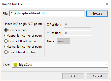
Once inside Pcbnew, we want to import the heart shape we created into the edge layer. As mentioned above, this layer will define the shape of the board, and any cuts we want to make into it. To import our heart shape, we select “File” -> “Import” -> “DXF File” and choose the heart.dxf file we previously created.
Then choose the “Edge.Cuts” layer, and click “OK”:
You should now see the heart in KiCad’s Pcbnew:

Now we can move on and add the other layers in Inkscape. For this project, we will add two layers: a copper layer, which will cover most of the board, give us a nice round border (by slightly changing the shade of the Solder mask layer above it, as explained before), and give us the shiny gold plating for the keyhole and text, and a solder mask layer.
The Copper Layer: Add Some Artistic Flair!
Let’s start with the copper layer. Select the heart shape, click “Ctrl+D” to duplicate it, and then Ctrl+J (or “Path” menu -> “Dynamic offset”) and drag the small handle at the top of the heart inward to create a slightly smaller version of the heart. I used a lighter shade of purple for this layer:

Finally, convert the newly create object to path using “Ctrl+Shift+C” (or “Path” menu->”Object to Path”), flatten Beziers, and with the heart shape selected, click “Ctrl+Shift+N” (or “Layers” menu -> “Add Layer…”) and name the layer “Cu”. This stand for the Copper layer.
The Solder Mask: Including Text
Next, we are going to add the text, using the solder mask layer. This might seem counter-intuitive, but the solder mask layer actually specifies which parts of the board will not be covered by solder mask (it is also sometimes called “Stop mask” for that reason).
When you create electronics PCB, you usually want to cover everything by default, and only specify explicitly the parts you want to be exposed. In our case, we want the text to be exposed — that is, to just show the gold plated copper, without the solder mask covering it. Since we created the copper layer and it covers the entire area, we know this area will be covered with copper.
I used golden color for the Mask layer in InkScape, as it actually represents the areas of exposed copper. What color you pick doesn’t matter here, but it makes sense to use realistic colors so we get a good idea of what the board will look like.
To add text, we use the text tool — you can press “T” and then click anywhere to add the text. Use a font and style of your liking (I went with a free font called “Marketing Script”). You can use Inkscape “Align and Distribute” tool (find it instead the “Object” menu) to automatically align the text with the heart’s center.
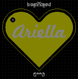
Once we got the text in place, we need to convert it into a path (“Path” menu-> “Object to Path”), then flatten Beziers just like we did with the heart shape above. Finally, we’d need to add the text into the Mask layer. Select it, press “Ctrl+Shift+N”, and type “Mask”. This is what the final result looks like in Inkscape:

Save the file as heart.svg, and you are ready to covert to a KiCad Footprint.
Making a Footprint
A Footprint is basically a unit that can be placed into PCB. We will use a free tool called svg2mod, which you can download here. You will also need to have Python 2.7 installed in order to run the script.
Run the script inside the KiCad project’s folder, giving it the input SVG and output file names:
python svg2mod.py -f 0.93 -i heart.svg -o heart.pretty/heartThe -f 0.93 option scales the file by a factor of 93%. I am not sure why it is needed, but otherwise you get the imported footprint slightly bigger than design. If you happen to figure out why this is, please let me know :-)
The output should look similar to this:

Look for the Found SVG layer: CU and Found SVG layer: Mask lines which indicate that svg2mod.py was able to find the relevant layer files.
If svg2mod.py is taking long time to run (it shouldn’t take more than 2–3 seconds), it means you have some paths that you need to apply the “Flatten Beziers“ option on, as explained above.
Next, we need to import this footprint into our KiCad project. In Pcbnew, go to “Preferences” -> “Footprint Libraries Wizard”, in the dialog choose “Files on my computer”, hit “Next”, then choose the heart.pretty directory inside your project directory. Click “Next” to select the file, and then click “Next” again to confirm the import, and finally, choose to import it “To the current project only” (unless you want to reuse the footprint in other KiCad projects).
Now you can add the footprint to your PCB — Click on the “Add footprints” button in the right toolbar:

and then click somewhere inside the heart shape. When you see the “Load Footprint” dialog, type heart:heart and enter to load the heart footprint. You can click on “Select by Browser” and find the footprint in the catalog.
Now we’re ready place the footprint into the PCB design. You can use the Ctrl+Shift key combination while moving the footprint to disable snapping it to the grid. The result should look similar to this:

Don’t worry about the gray svg2mod text — it won’t appear in the final PCB.
Adding a Keyring Hole
One final piece we are still missing is a small hole for mounting. Since I intended this to be a keychain light, I put hole in one of the sides of the heart. If it were a pendant, then a hole in the center would probably make more sense.
To add our mounting hole, we’ll use a preset footprint in KiCad.
Click the “Add Footprints” button and add a footprint called Wire_Pads:SolderWirePad_single_2mmDrill . This footprint contains a single, round, 2mm copper plated hole. Place this footprint where you want the hole to be, and then right click on it and select “End Tool”. Then, move the cursor over the newly added pad footprint, press “E”, and choose “Footprint REF** on F.Cu”. This will open a dialog where you can edit the footprint parameters — we’ll Edit the Ref property, and remove the text so it won’t appear on our Silk Screen of the final board:

You can also remove the “Value” of the footprint in a similar fashion.
Finally, you can adjust the hole diameter and the brim size by moving your cursor over the pad again, pressing “E” and choosing “Pad 1 on F.Cu, B.Cu, Internal, Non-copper of”.
Set “Size X” on the left to be the perimeter you want for the hole and the drill (I used 2.6mm) and the “Size X” inside “Drill” pane to be the perimeter of the actual hole (I used 2mm):

Once you are done with the steps above, you should see the hole appear on your design:

At this point, you can also add some electronic components on the back side of the board— I added a button cell battery holder, 5 LEDs, a switch, and a resistor to create a small key chain light. But the electronic part is out of the scope of the tutorial — we’ll focus only on the art. For now, we will simply duplicate the artwork to the back side of the PCB — simply add the heart:heart footprint again, and then press “F” to move it to the back size of the board. This will also flip it, so press “R” twice to rotate it back to the original orientation. Finally, place it over the front image — use Ctrl+Shift for accurate placement. The end result should look similar to this:
If you’d like to try your hand at including the circuitry in your board, I’ve uploaded a KiCad project with the electronics footprints included to my github.
Checking Our Work
KiCad has a really nice feature to render a 3D model of your board. This is really useful in understanding what the result will look like. Press “Alt+3” inside Pcbnew to open the 3D View (you can also open it through “View” menu -> “3D Viewer”).
Inside the 3D Viewer, enable the Realistic Mode, and set the colors of the Solder Mask and Copper/Surface Finish to the colors you will actually use to get a good idea of what the final board will look like. I used purple for the Solder Mark, and golden yellow for the finish, as I will choose the ENIG finish (= gold plated copper).
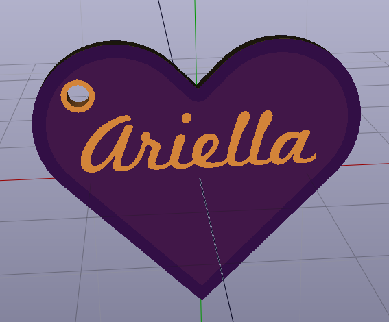
You can find the final KiCad project file and the SVG file that I created for this project here: https://github.com/urish/heart-ariella/tree/master/kicad
Choosing a Manufacturer
Congratulations! You have successfully turned your artwork into a PCB plan, and now you are ready to send it to manufacture. There are plenty of options, but here are two of my favorites:
OSH Park — Choose them if you want a purple board with gold (ENIG) copper finish. There is no color choice for the board/mask, but the quality is excellent, and the prices are pretty competitive for smaller projects, especially given the free international shipping. You get 3 copies of the board, which are shipped in about two weeks.
One of the nice things about OSH Park is that you can upload your KiCad PCB file directly, and instantly get a preview of what the final board will look like and a quote based on the dimensions of the PCB. The quality is excellent and they are my go-to place for smaller boards with purple color. They are based in the US.

Pcbway — This is a Chinese factory with fast turnaround times and a wide selection of options for an affordable price. The basic deal includes 5 or 10 copies of your PCB for any size up to 10x10cm, with the default options for just 5$ + shipping. Most of the silk screen colors are included for the basic deal. If you want a lead-free process, then you will have to pay more though — 18$ for solder finish, or 38$ for gold (ENIG finish). They usually manufacture and ship the boards within 3–4 days, and you can follow the manufacturing process for your order on their website.
You can get an instant online quote here. Don’t be intimidated by the number of options — the import things to fill in are the dimensions of the board (don’t worry about being accurate here — a ballpark is fine too, they will fix it after you upload the files), the quantity — 5 or 10 are usually for the same price, and you can’t order less than 5, then choose the color of the Solder Mask, and optionally change the Finish Type to HASL Lead Free (that’s tin plated, but without lead) or Immersion Gold. You can leave everything else set to the defaults.
Note that Pcbway will add the order number on your front Silk Screen layer — you can see that at the bottom of the Panda PCB. I noticed they will usually place it in a place that makes sense so as to not ruin your design. Also, they will review your design and approve it (usually within a few hours), and only then you will be able to pay for the order and manufacturing will begin. If there is a problem with your files, they are likely to contact you by email and ask you how to proceed.
Another alternative is seeedstudio.com — they have similar deal as PCBWay, but PCBWay has more Solder Mask options and faster turnaround times, so I usually prefer them.
Finally, if you really want to stretch your money, you can go to pcbshopper.com, which compares prices over 25 different PCB manufacturers.
Preparing Your Files for Manufacturing
When you wish to export your project files from KiCad for manufacturing, you need to use a format called Gerber. All manufacturers should accept this format. To export the project, simply go to “File” menu-> “Plot”, and make sure the settings match the screen shot below:
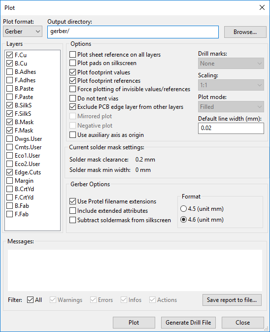
These are the settings I used when manufacturing the Panda PCB through PCBWay. Click on “Plot” and then also “Generate a Drill File”. Make sure that the Drill Units are set to Millimeters, and select “Protel” in “Drill Map File Format”. Finally, click on “Drill Files button”:
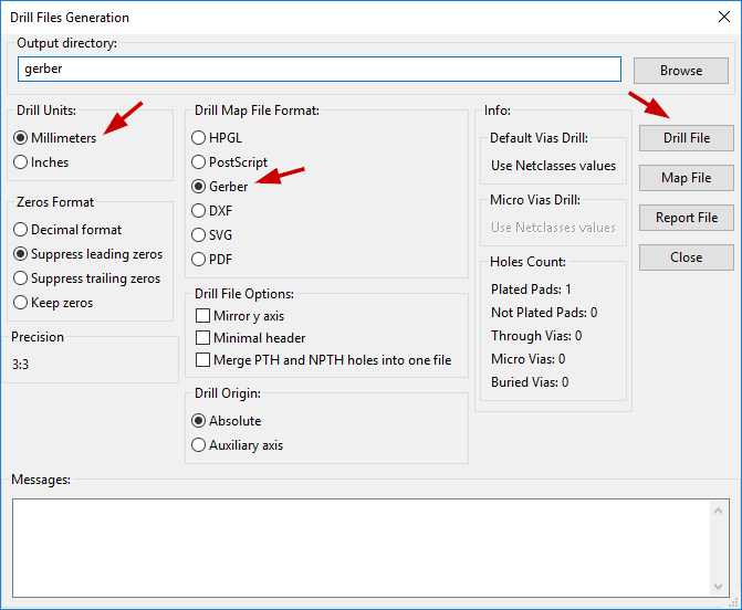
After following these steps, you should find 8 files in the output directory. Zip them together and upload them to the manufacturer site. I suggest also using the free online gerber-viewer.com service to visually inspect the and validate files — just upload the ZIP file there and you will be able to view all the different layers, as they will be manufactured:

You can also upload the Zip file to OSH Park for visual inspection. In fact, I do this all the time :-)
Send Files to the Manufacturer, a Short Wait, and Then…
Your PCBs are ready to go! You can now solder in any components you included wiring for, and then you’re all set to enjoy the fruits of you hard work:

Making the Panda
For the panda PCB, the process is very similar, but I also used the Silk Screen layer. If you use it in your project, simply call it “SilkS” in inkscape. You can find the full list of KiCad layers and their respective names in Inkscape here.
You can find the Panda’s original SVG here, and also the SVG with all my modifications, split into layers and ready to export to KiCad. This what it looks like in Inkscape:

And in KiCad:

Conclusion
As I mentioned in the beginning, making your own PCBs is a great way to customize and improve your home electronics projects, but on top of that, making them more “artistic” and adding visual designs to them only adds to the fun (and boosts their “giftability” ;-). Even if you decide not to go artwork-crazy, hopefully this tutorial helped you better understand how PCBs are made so you can have a better appreciation for the great work they do for custom electronics.
What will you build?
Now go ahead, build cool things, and please share what neat things you’ve made in the comments!